
The major research directions include
If you have resolved to devote yourself to IC field … AND
If you are desperately striving for excellence and pleased to face work that is challenging and creative …
JUST JOIN US!
|
|
|
||||||||
|
|
|||||||||
|
|
The major research directions include |
||||||||
|
|
Fabrication of high-performance Ge-based devices on Si substrate 矽晶圓上高效能鍺元件之開發 | ||||||||
|
|
Research on crystalline high-κ dielectric for Si-based devices 結晶態高介電材質於矽基元件應用 | ||||||||
|
|
Development of high density MIM (metal-insulator-metal) capacitors 高品質金屬-絕緣層-金屬電容之開發 | ||||||||
|
|
Process development of high-efficiency Si-based solar cells 高效率矽晶太陽電池製程 | ||||||||
|
If you have resolved to devote yourself to IC field … AND If you are desperately striving for excellence and pleased to face work that is challenging and creative … JUST JOIN US! |
|||||||||
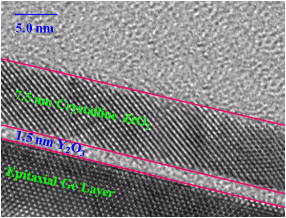
Fabrication of high-performance Ge-based devices on Si substrate
 Ø
Despite great advancement in high-κ gate
dielectrics, metal gates and strain engineering, the effort to pursue devices
with higher performance never slows down. Due to the superior carrier mobility
against Si, germanium (Ge) has received much attention and been regarded as a
potential channel material to accommodate the ever-stringent scaling requirement
for future technology nodes. Recently, the research on Ge-related technology has
drawn intense attraction which can be evidenced by independent sessions in
prestigious conferences or even independent conferences for the topic. Based on
the process of forming an epitaxial Ge
layer on Si substrate, our
research team continues to explore new approaches to fulfill Ge devices with
higher performance.
Ø
Despite great advancement in high-κ gate
dielectrics, metal gates and strain engineering, the effort to pursue devices
with higher performance never slows down. Due to the superior carrier mobility
against Si, germanium (Ge) has received much attention and been regarded as a
potential channel material to accommodate the ever-stringent scaling requirement
for future technology nodes. Recently, the research on Ge-related technology has
drawn intense attraction which can be evidenced by independent sessions in
prestigious conferences or even independent conferences for the topic. Based on
the process of forming an epitaxial Ge
layer on Si substrate, our
research team continues to explore new approaches to fulfill Ge devices with
higher performance.
The main research contents include
(A) Passivation of Ge surface (鍺層表面鈍化)
(B) Integration of crystalline high-κ dielectrics into Ge MOS devices (結晶態高介電材質與鍺MOS元件之整合)
(C) Fabrication of nonvolatile memory on Ge layer (製作鍺為基礎之非揮發性記憶體)
Research on crystalline high-κ dielectric for Si-based devices
 Ø
Because of possessing relatively higher
κ value than their amorphous counterparts, tetragonal/cubic ZrO2 and
HfO2 have aroused considerable interest in the IC industry. Besides
applying tetragonal ZrO2 to aforementioned Ge-based devices, our
research team has also
dedicated to the integration of
promising crystalline high-κ
dielectrics
into Si-based devices. In addition, we
successfully master the technology to control the concentration
of oxygen vacancies in the crystalline high-κ dielectrics by modulating process
parameters. Dielectrics with low and high concentration of oxygen vacancies can
be respectively applied to gate dielectrics for MOS devices and charge trapping
layer for flash memory devices. We are one of the pioneering research teams in
the world focusing on the application of crystalline high-κ dielectrics to
electronic devices.
Ø
Because of possessing relatively higher
κ value than their amorphous counterparts, tetragonal/cubic ZrO2 and
HfO2 have aroused considerable interest in the IC industry. Besides
applying tetragonal ZrO2 to aforementioned Ge-based devices, our
research team has also
dedicated to the integration of
promising crystalline high-κ
dielectrics
into Si-based devices. In addition, we
successfully master the technology to control the concentration
of oxygen vacancies in the crystalline high-κ dielectrics by modulating process
parameters. Dielectrics with low and high concentration of oxygen vacancies can
be respectively applied to gate dielectrics for MOS devices and charge trapping
layer for flash memory devices. We are one of the pioneering research teams in
the world focusing on the application of crystalline high-κ dielectrics to
electronic devices.
The main research contents include
(A) Crystalline ZrO2 as the gate dielectric of MOS devices (以結晶態ZrO2應用於MOS元件之閘極介電層)
(B) Crystalline ZrO2 as the charge trapping layer of flash memory devices (以結晶態ZrO2應用於快閃記憶體之電荷陷阱層)
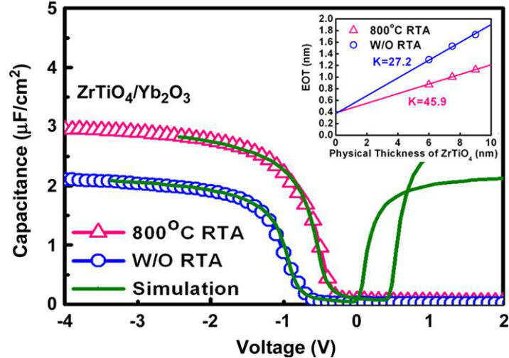
Development of high density MIM (metal-insulator-metal) capacitors
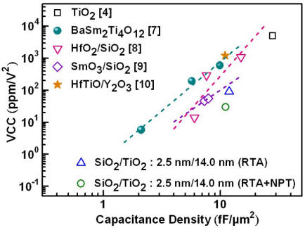
Ø MIM capacitors have been employed in a wide variety of electronic applications such as dynamic random access memory (DRAM), analog integrated circuits, and radio frequency (RF) circuits. As the technology advances, the ever higher capacitance density, lower leakage current as well as better reliability are required to facilitate the downscaling of the devices. To achieve this goal, many high-κ dielectrics have been investigated. In the past few years, our research team has successfully accomplished high-performance MIM capacitors by employing crystalline high-k dielectrics or some novel amorphous dielectrics as the insulator. Based on the results, we will continue investing in the development of innovative processes and materials to fulfill MIM capacitors with higher performance.
Process development of high-efficiency Si-based solar cells
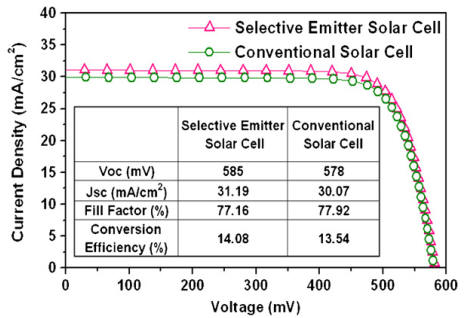 Ø
A high
conversion efficiency coupled with a low production cost is the key factor to
popularize photovoltaic energy conversion. In a conventional
Si-based crystalline solar cell, the emitter structure has a homogeneous doping
profile and low sheet resistance (45-55 Ω/sq) to obtain low contact resistance
and prevent metal penetration through the junction during the co-firing process.
However, the emitter structure must be modified to obtain higher conversion
efficiencies, since a highly doped emitter restricts the surface passivation and
the response to short wavelength light, while increasing the surface
recombination losses.
A selective emitter
that features lightly doped regions between the metal grids and heavily doped
regions underneath the metal contact has been widely
perceived as one of the most promising
structures to realize high-efficiency cells.
A
single phosphorus diffusion has been developed through the selective thin SiNx
film formed by NH3 plasma nitridation of the Si surface by our
research team. In the next step, some down-conversion techniques will be
integrated into our solar cells to further enhance its efficiency.
Ø
A high
conversion efficiency coupled with a low production cost is the key factor to
popularize photovoltaic energy conversion. In a conventional
Si-based crystalline solar cell, the emitter structure has a homogeneous doping
profile and low sheet resistance (45-55 Ω/sq) to obtain low contact resistance
and prevent metal penetration through the junction during the co-firing process.
However, the emitter structure must be modified to obtain higher conversion
efficiencies, since a highly doped emitter restricts the surface passivation and
the response to short wavelength light, while increasing the surface
recombination losses.
A selective emitter
that features lightly doped regions between the metal grids and heavily doped
regions underneath the metal contact has been widely
perceived as one of the most promising
structures to realize high-efficiency cells.
A
single phosphorus diffusion has been developed through the selective thin SiNx
film formed by NH3 plasma nitridation of the Si surface by our
research team. In the next step, some down-conversion techniques will be
integrated into our solar cells to further enhance its efficiency.