|
|
|
 |
| |
|
|
 |
 |
| |
 |
|
Personal vehicles have shifted from fuel to
hybrid/electric power in pursuit of reduced
carbon emission due to the increasing awareness
of environmental protection. Power modules have
become a crucial component of modern-day
electric vehicles (EVs) considering the
increasing demand for high power and voltage
output. However, the direct bonded copper
substrate in the traditional power module still
has warpage issues after the manufacturing
process. This phenomenon leads to poor heat
dissipation after assembly with heat sink due to
high switching speed with large heat generation
rates within the components, which eventually
fails to meet the requirements of modern-day
EVs. Additionally, mechanical and thermal issues
will affect the reliability of power modules.
Therefore, establishing a process-oriented
simulation methodology, which considered the
coupling effect of thermal and electrical
responses to improve the mechanical behavior,
and optimizing the reliability of the IGBT
high-power module, are crucial topics in the
current research. |
|
 |
|
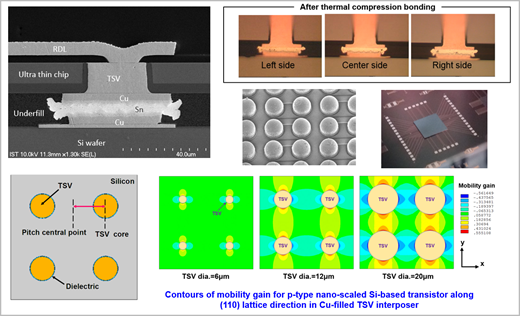
Fig.1 Fabrication, wafer level assembly,
simulated analysis of ultra thin chip of 3D ICs. |
|
 |
|
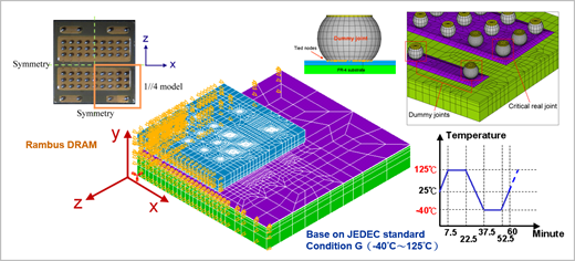
Fig.2 Finite element model and
simulation of advanced packaging architecture. |
| |
|
 |
|
Packaging technology has gradually developed
toward minimized dimension, high I/O count, and
multi-chip integrated architecture. Fan-out
panel-level packaging (FOPLP) has currently
become the most popular packaging technology
because it has the highest potential to overcome
the previously mentioned difficulties. However,
several concerned mechanical characteristics,
such as the coefficient of thermal extension
mismatch induced from heterogeneous integration
and heat and chemical reactions of the molding
compound, would result in serious warpage issues
during the manufacturing process of FOPLP. Such
issues would eventually lead to packaging
reliability deterioration. Thus, the macroscopic
and microscopic physical behaviors of material
models used in the simulated analysis should be
carefully considered to resolve the significant
dimension mismatch within the components of
actual FOPLP vehicles. Investigations on
advanced packaging techniques based on the
summary of the aforementioned challenges would
be the next considerable leap among the research
topic of mechanical engineering. |
|
 |
|
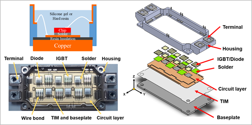
Fig.3 Power module with insulated metal
substrate (IMS). |
|
 |
|
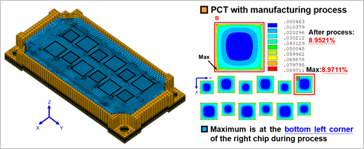
Fig.4 Finite element model & equivalent
plastic strain distribution of IMS module under
PCT. |
| |
|
 |
|
Along with the innovated film materials,
flexible electronics has rapidly grown among
wearable devices with the advantages of light
weight, minimized thickness, and applicability
on various shapes and sizes. The specific
feature of flexible and foldable electronics
lies in the capability to withstand repeated
loadings under a few millimeters of bending
radius. The soft device has various
applications, such as wearable device, curved
display, flexible solar cell, and printed
electronics. Additionally, the most crucial part
of flexible display includes flexible glass,
metal foils, and polymer films. Particularly,
flexible glass has outstanding optical
applications and low thermal extension
coefficient and could be adopted as a barrier to
prevent vapor and air from entering the package.
However, flexible glass also has the
disadvantages of fragility, increased production
cost, and high restrictions on applied bending
radius. Therefore, the locations of multiple
neutral axes should be seriously considered to
prevent the flexible glass from fracture. The
number and positions of the neutral axes can be
appropriately configured with the mechanical
model and analytic results presented in this
research. This configuration is expected to be
an important design reference for the
next-generation soft electronic architectures. |
|
 |
|
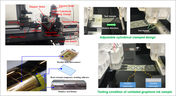
Fig.5 Actual measurement platform
utilized in the mechanical loading tests of
flexible hybrid electronics (FHE). |
|
 |
|
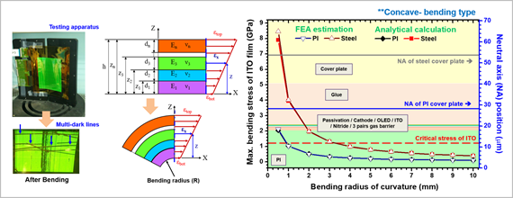
Fig.6 The screen of OLED flexible
display appears multi-dark lines induced by
testing apparatus with thousands bending
performance. Also, strain distribution of
flexible display is derived based on the
schematic drawing. |
| |
|
 |
|
The
dimension of semiconductors has shifted from
micron to nanometer scale due to the rising
demand for high performance on electronic
devices. However, the conventional method of
shrinking the device by decreasing the
characteristic dimension (length and width) of
the actual device has led to some bottlenecks in
manufacturing. An alternative way is to utilize
the advantages of 3D structures, including
FinFET and gate-all-around FET, to improve the
controllability and performance of the
semiconductor device. Additionally,
process-induced performance enhancements, such
as gate-last, high-k metal gate novel
semiconducting materials (SiGe, Ge, and III-V),
and strain engineering, can boost the overall
performance of the device. In the evolution of
semiconductor architecture, the technology node
is used as a description of the generation for
the semiconductor device, while the 22 nm
technology node was regarded as the final
chapter of the planar device. Novel techniques
in 7 nm FinFET and 3 nm GAA-FET have been
observed to be candidates due to improved
electrical performance. Thus, the possibility of
strain engineering to obtain further boost is
regarded as a novel topic in the semiconductor
industry. |
|
 |
|
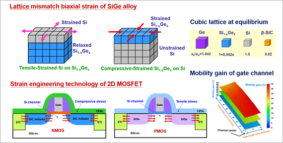
Fig.7 Mechanism of induced lattice
mismatch stress within 2D MOSFETs and the
schematic diagrams of preferred stress
components in N/P MOSFETs. |
|
 |
|
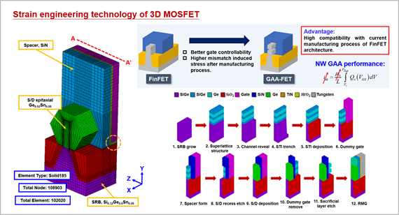
Fig.8 Process-oriented device simulation
considered in advanced 3D MOSFETS. |
| |
|
 |
|
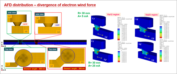
For the next generation of integrated circuits,
the copper/low-k interconnect system has the
advantage of reducing RC delay between adjacent
lines and connections, thereby minimizing the
energy consumption. Therefore, this system is
regarded as the best solution to interconnect
materials for current advanced chips. Along with
the decreasing dimension from micron to
nanometer scale, the emerging difficulties in
reliability and failure mechanisms with the
reduction of interconnection width and the
geometry variation in the circuit must be
urgently studied. The major issues of
electromigration (EM) will lead to void growth
inside the copper line. Moreover, the
interconnect comprising different materials
suffers from a mismatch considering the thermal
expansion coefficient, which drives the vacancy
from grain boundaries to via area due to stress
gradient. This phenomenon eventually causes
component failure, which is also known as the
stress migration (SM) effect. By contrast,
reliability problems regarding interfacial
fractures in bonded interfaces between low-k
materials and barrier layers should be carefully
considered with the application of external load
or process-induced stress. Therefore, the
current research focuses on the reliability
physics and failure mechanism as well as the
impacts of scaling sizes and geometry variations
for interconnects. Moreover, the next-generation
interconnect system, including novel processes
and new materials, will be comprehensively
explored and discussed. |
|
 |
|
Fig.9 Simulation investigation of
nano-scaled interconnect reliability by using
Atomic Flux Divergence (AFD) based approach. |
|
 |
|
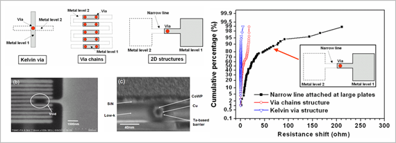
Fig.10 A new stress migration failure
mode in highly scaled Cu/Low-k interconnects. |
|
|
| |
|
|
|
|
| |
|
|
|